



LM
Luis Minvielle
Where To Find Software Engineering Jobs
over 2 years ago
Ist dies Ihr nächster Job Lesen Sie die vollständige Beschreibung unten, um dies herauszufinden, und zögern Sie nicht, sich zu bewerben. tomorrow’s technology.
IoT, 5G and Artificial Intelligence. Unthinkable without us. More than half of all the microchips produced worldwide first pass through our hands. As the global market leader of automated test systems in the semiconductor industry we help the world to realize the digital transformation, enable our customers to shape the future and offer you the exciting jobs intended for pioneers.
Are you seeking answers and opportunities for your future? At our site in Böblingen you will find both as
Test Solution Engineer - Research & Venture (m/f/d)
Your Responsibilities Develop and prototype innovative semiconductor test solutions and methodologies for emerging technologies and applications. Validate and implement new test concepts on the Advantest V93000 platform, from feasibility studies through proof-of-concept demonstration and customer engagement. Collaborate with customers, technology partners, and internal organizations to identify and address future test challenges Work across Advantest business units to accelerate innovation and solution development Contribute to the generation of intellectual property, technology demonstrators, and future product concepts Analyze industry trends and help define the next generation of semiconductor test solutions
Master’s Degree or PhD in Electrical Engineering, Physics, Mechatronics, Microelectronics, Semiconductor Engineering, Computer Engineering, Microsystems Engineering, Materials Science, or a related technical discipline. Demonstrated professional hands-on experience on the Advantest V93000 platform and Smartest 8 environment with a focus on high-speed, RF or electro-optical applications Demonstrated professional experience in PCB design for DUT boards and probe cards, with a focus on high-speed applications Strong knowledge of high-speed digital interfaces, such as PCIe, UCIe, Ethernet, USB, or CXL, and measurement techniques Solid understanding of semiconductor devices, advanced packaging, test methodologies, and electronic measurement principles. Interpersonal Skills: Strong collaboration abilities across diverse teams, cultures, and organizational levels. Strong aptitude in creative thinking and problem-solving. Excellent communication skills; fluency in English is required, German is preferred. Willingness to travel occasionally up to 20%.
Our offer Flexibility Benefits Development Fitness Security Flexible and trust-based working hours, 30 vacation days + option for additional vacation days, mobile working, individual part-time models and programs for extended periods of absence Attractive salary, share in Advantest ́s success through our exceptionally appealing bonus program as well as numerous subsidies, discounts and offerings (e.g. bike leasing) Structured onboarding programs and mentoring, development discussions, technical and soft skill trainings, language courses and knowledge sessions Ergonomic working environment, sports and fitness options and events (e.g. Global Challenge) as well as health days Attractive company pension scheme, comprehensive insurance coverage and support in emergency situations
This job is hosted externally. Click below to view the full posting and apply.
Talks and stories from around this role — technically off-topic, practically not.
4:52 min
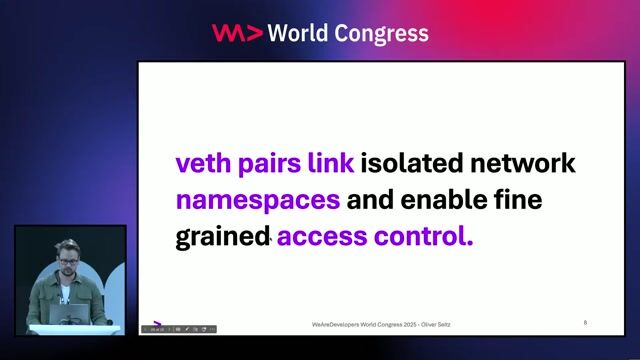
 Oliver Seitz · World Congress 2025
5:24 min
2:50 min
2:12 min
1:34 min
2:58 min
.webp)
.webp)
.webp)