




Semiconductor application engineer
- Discuss this with your agent
- Open in Claude
- Open in ChatGPT
Prepare application
- Draft this with your agent
- Open in Claude
- Open in ChatGPT
Role details
Tech stack
Job description
We are looking for a Semiconductor Application Engineer. You will work at the intersection of chemistry, materials science, wafer processing and customer applications, helping semiconductor manufacturers successfully evaluate, qualify and optimize advanced materials within their production processes.
This is an excellent opportunity for a Process Engineer, Lithography Engineer, R&D Engineer or Application Engineer who enjoys combining experimental work with technical problem-solving and customer interaction.
- Providing technical product and application support to customers in the semiconductor industry.
- Supporting the evaluation, qualification and optimization of electronic materials used in advanced wafer-processing applications.
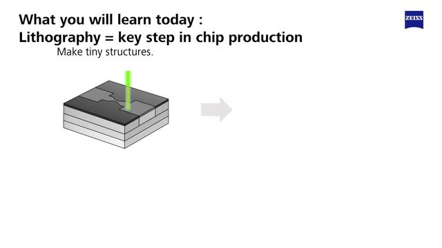
- Setting up and coordinating experiments in the application laboratory, with a strong focus on photolithography and coat/exposure/develop processes.
- Analysing experimental and process data and translating your findings into clear technical recommendations for customers.
- Investigating technical issues and supporting customers with troubleshooting and process improvement.
- Working closely with internal teams such as R&D, Quality, Production, Product Management and Sales, as well as international technical experts.
- Preparing and presenting technical reports, application data and presentations for customers and internal stakeholders.
- Contributing to the qualification and optimization of laboratory equipment and analytical methods, while keeping up with new developments in semiconductor technology.
Requirements
- A Masterâs degree in Chemistry, Physics, Materials Science, Engineering.
- Experience with experimental research or process development.
- Several years of professional experience within semiconductor processing, preferably in a wafer fab, semiconductor company or research environment.
- A good understanding of semiconductor manufacturing and wafer-processing technologies.
- Experience with photolithography, particularly processes such as coat, exposure and develop, is a strong asset.
- Experience with areas such as photoresists, developers, wet chemistry, thin films, cleaning processes or electronic materials can be highly relevant.
- You can occassionally travel abroad to attend conferences or meet with clients (sporadic frequency).
Benefits & conditions
- Competitive salary tailored to your experience.
- Meal vouchers at the maximum amount.
- Group insurance.
- Hospitalisation insurance.
- Dental insurance.
- CAO 90 bonus.
- Flex Income Plan.
- Possibility of bicycle leasing through the Flex Income Plan.
- Possibility to purchase multimedia equipment through the Flex Income Plan.
- Possibility to choose a DeWaterbus subscription through the Flex Income Plan.
- Possibility to obtain an electronic toll badge through the Flex Income Plan.
- 20 statutory holidays.
- 15 additional ADV days.
- Seniority vacation days.
- Flexible working hours.
- On-the-job training.
You will join a large and stable international organisation that will further immerse you in the world of fine chemicals and micro- and nanoelectronics. It is an excellent environment to deepen your expertise, gain exposure to advanced technologies and take the next step in your professional career.
Apply for this position
This job is hosted externally. Click below to view the full posting and apply.
Prepare application
- Draft this with your agent
- Open in Claude
- Open in ChatGPT
Good distractions
Talks and stories from around this role â technically off-topic, practically not.
Moments
Explore playlistsVideos
See allRelated articles
See all
Where to Find Entry-Level Software Engineering Jobs
Best Companies in the Netherlands: Top 25 Companies in 2023Â
How to land a developer job in Amsterdam
Software Developer Salary in The Netherlands [2023]